

Department of Physics and Astronomy: Publications and Other Research
Sy-Hwang Liou Publications
Document Type
Article
Date of this Version
4-15-1995
Abstract
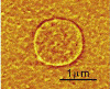
Sm-Co film is a potential candidate for the future high density recording media of 10 Gb/in2 which requires bit sizes of the order of 300 nm and grain sizes of about 10 nm. This article investigates the microstructure of the Cr underlayer in Sm-Co thin films and its effect on Sm-Co thin films prepared by the dc magnetron sputtering technique. The grain size of the Cr underlayer is found to be about 25 nm. Grains with small angle misorientation usually form local agglomerates. Studies by transmission electron microscopy (TEM) bright field images at different defocus settings and by high resolution electron microscopy indicate that a large proportion of the grain boundaries have gaps. The gap width (about 1–3 nm) varies from place to place. The Sm-Co films deposited on the Cr underlayer inherit similar gaps at positions adjacent to the grain boundary gaps of the Cr underlayer. Such gaps produce grain-like contrast of about 25 nm in TEM bright field images. However, such contrast becomes weak as the thickness of the film increases and disappears at a thickness of 96 nm, suggesting the gaps are sealed at places far from the Cr underlayer. The effect of the Cr underlayer on magnetic properties are discussed.
Comments
Published by American Institute of Physics. J. Appl. Phys., 77, 3831(1995). © 1995 American Institute of Physics. Permission to use. http://jap.aip.org/jap/.