

Department of Physics and Astronomy: Publications and Other Research
Peter Dowben Publications
Document Type
Article
Date of this Version
July 2003
Abstract
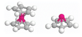
The present invention relates to the fabrication of a boron carbide/boron semiconductor devices. The results suggest that with respect to the approximately 2 eV band gap pure boron material, 0.9 eV band gap boron carbide (B5C) acts as a p-type material. Both boron and boron carbide (B5C) thin films were fabricated from single source borane cage molecules using plasma enhanced chemical vapor deposition (PECVD). Epitaxial growth does not appear to be a requirement. We have doped boron carbide grown by plasma enhanced chemical vapor deposition. The source gas close- 1,2-dicarbadecaborane (orthocarborane) was used to grow the boron carbide while nickelocene (Ni(C5H5)2) was used to introduce nickel into the growing film. The doping of nickel transformed a B5C material p-type relative to lightly doped n-type silicon to an n-type material. Both p-n heterojunction diodes and n-p heterojunction diodes with n- and p-type Si [1,1,1] respectively. With sufficient partial pressures of nickelocene in the plasma reactor diodes with characteristic tunnel diode behavior can be successfully fabricated.
Comments
Patent NO.: US 6,600,177 B2