

Electrical and Computer Engineering, Department of
P. F. (Paul Frazer) Williams Publications
Accessibility Remediation
If you are unable to use this item in its current form due to accessibility barriers, you may request remediation through our remediation request form.
Document Type
Article
Date of this Version
August 1992
Abstract
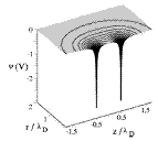
We present an optical technique for the measurement of semiconductor surface electric fields. The measurement technique uses the Kerr electro-optic effect in nitrobenzene, a phase sensitive interferometer, and associated data acquisition units to measure the surface electric fields between the contacts of a planar semiconductor device. This technique was used to measure the surface fields on silicon devices used in pulsed power applications, but has the potential for use as an electric field probe for any device having high surface electric fields, both pulsed and dc. The measurement technique showed a temporal resolution of 100 ns, which can be easily reduced to a few nanoseconds using superior data acquisition and detection systems. The spatial resolution was about 50 pm for devices that had a typical contact separation of about 500 pm (power devices). This technique can be applied to measure the surface fields on devices commonly used in microelectronic applications. In this paper we discuss in detail the measurement technique and present the results obtained for silicon photoconductive power switches.
Comments
Published in Rev. Sci. Instrum. 63 (8), August 1992. Copyright © 1992 American Institute of Physics. Used by permission.