

Department of Physics and Astronomy: Individual Faculty Pages
Peter Dowben Publications
Accessibility Remediation
If you are unable to use this item in its current form due to accessibility barriers, you may request remediation through our remediation request form.
Document Type
Article
Date of this Version
January 1996
Abstract
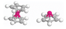
We have succeeded in the fabrication of a boron–carbide/boron diode on an aluminum substrate, and a boron–carbide/boron junction field effect transistor. Our results suggest that with respect to the approximately 2 eV band gap pure boron material, 0.9 eV band gap boron–carbide (B5C) acts as a p-type material. Both boron and boron–carbide (B5C) thin films were fabricated from single source borane cage molecules using plasma enhanced chemical vapor deposition (PECVD). Epitaxial growth does not appear to be a requirement. ©1996 American Institute of Physics.
Comments
Published Appl. Phys. Lett. 68 (1996) 1495-1497. Permission to use.